June 26, 2026 IBM says it has developed the world’s first functional sub-1 nanometre computer chip, marking what the company describes as a major advance in semiconductor technology. The company said the new chip architecture delivers twice the transistor density of its previous 2-nanometre design and could provide up to 50 per cent more performance or 70 per cent greater energy efficiency.
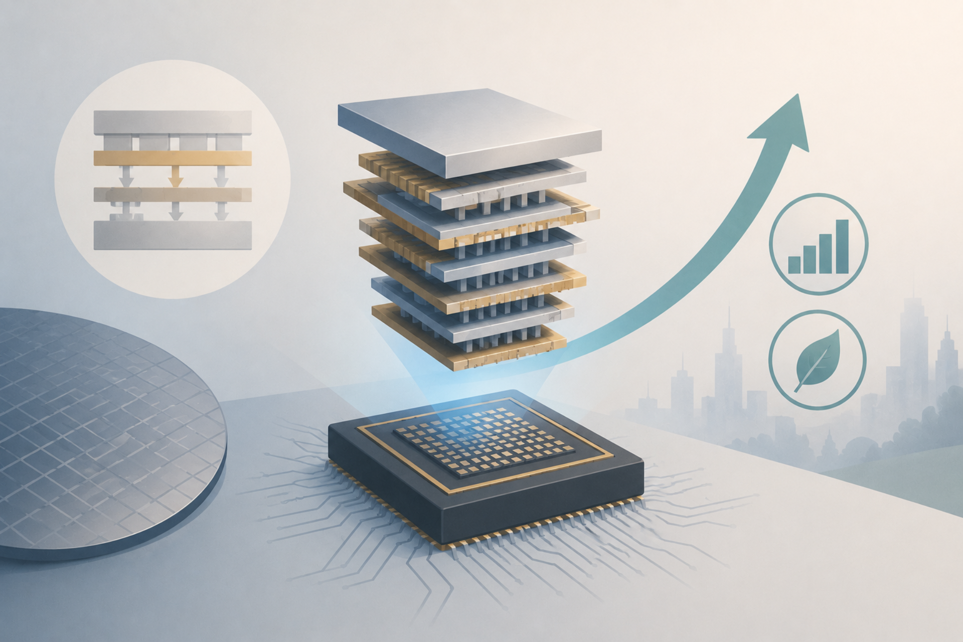
The technology is based on a new “nanostack” architecture that builds on IBM’s existing nanosheet transistor design, first unveiled in 2021 as part of its 2-nanometre chip research.
IBM said the new design enabled researchers to create a functioning 7-angstrom, or 0.7-nanometre, chip containing nearly 100 billion transistors on a chip roughly the size of a human fingernail. According to the company, the increased transistor density could allow future processors to deliver significantly greater computing power while reducing energy consumption.
Jay Gambetta, director of IBM Research, said the breakthrough could support a future in which computing performance continues to improve without a corresponding rise in power use. “The new architecture would enable a future where computing becomes significantly more powerful without a corresponding increase in energy,” Gambetta said.
The nanostack approach vertically stacks and staggers nanosheet transistors to increase density. IBM said each transistor consists of three nanosheet elements approximately five nanometres thick, separated by gaps of about nine nanometres. The company said each nanosheet contains only 15 rows of silicon atoms.
Per the company’s estimate, it will take approximately five years before chips based on the nanostack architecture enter mass production.
The timeline comes as Japanese chipmaker Rapidus, which partnered with IBM to commercialize its existing nanosheet technology, aims to begin large-scale production of 2-nanometre chips in the second half of 2027.
IBM said additional details regarding commercialization plans will be announced in the future.

